PCB CAD layout service
Do you have a design in hand, a BOM and a schematic but no layout resource in-house? We have dedicated layout resources to help you put together the perfect printed circuit board for your requirements.
Do you have a design in hand, a BOM and a schematic but no layout resource in-house? We have dedicated layout resources to help you put together the perfect printed circuit board for your requirements.
We provide a range of technical support options, covering everything from simple PCB CAD layout to the electronic design of complex systems. Our multi-skilled teams have years of experience in using high-quality PCB CAD software and will offer comprehensive design advice to ensure that your printed circuit boards come to life in the best way possible.
As one of the UK’s most well-respected PCB manufacturers, we have spent over 60 years specialising in all aspects of the printed circuit board design process, offering superior PCB CAD layout, PCB fabrication and PCB assembly services to all our clients. Get your project on track and ready for production, and contact us today.
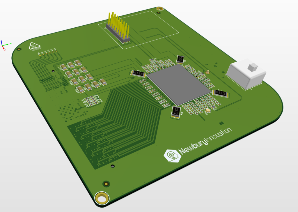
Computer-aided design, or CAD, is a vital tool in the creation of PCBs.
Using PCB CAD design software will create a perfect board layout and eliminate production and reliability problems. Newbury Electronics offers a pure PCB CAD layout support service to customers who:
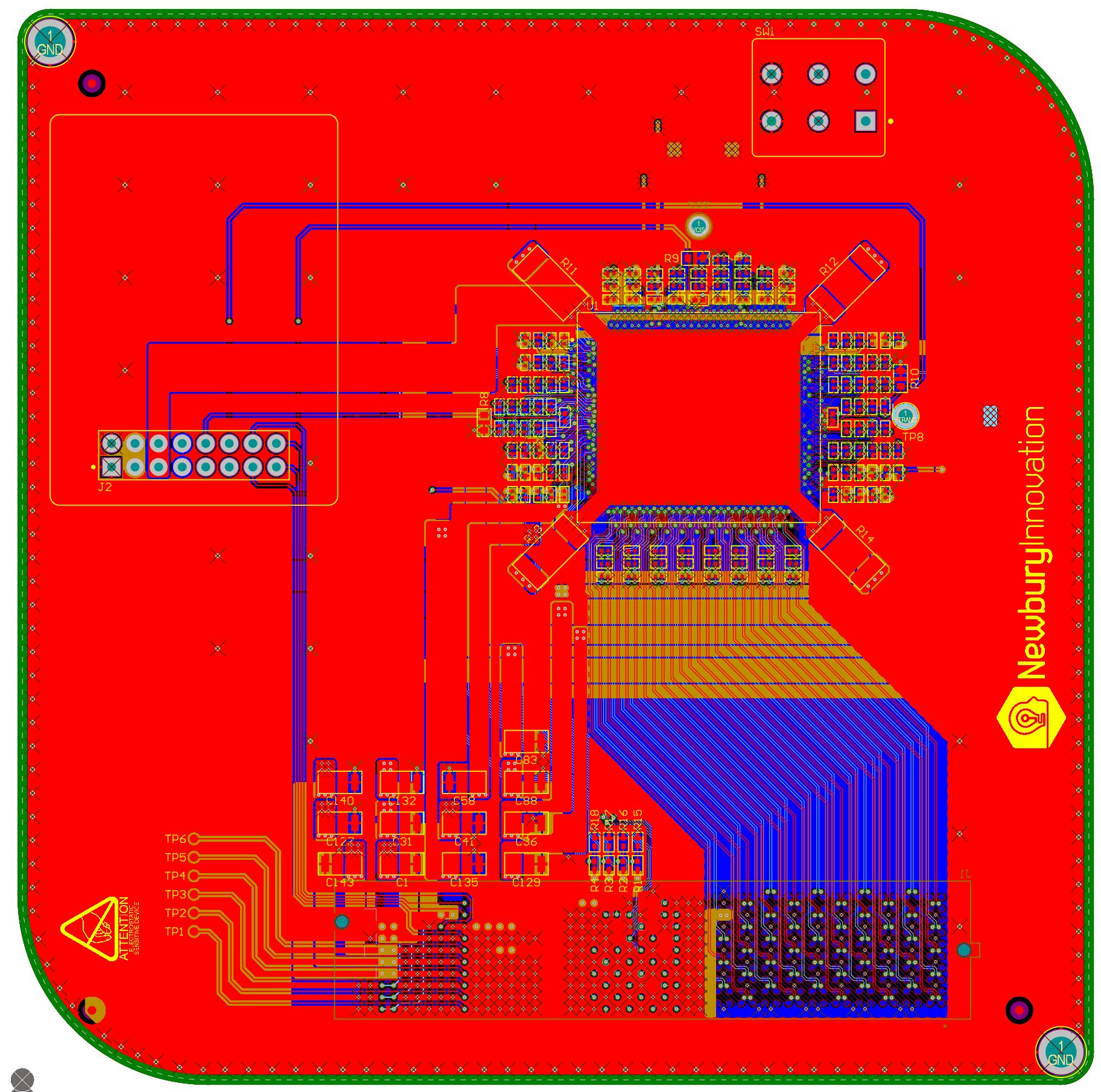
We will support the design & manufacture of everything from one-off prototypes to high-volume production loads. Whether your board is simple or complex, we’re equipped to deal with PCB design, fabrication & assembly for a range of applications across multiple industries, including Aerospace (AS9100 certified Assembly), wearable electronics and more. Read More
Our PCB designs comply with IPC-2581, IPC-2221, IPC-4101C, and IPC-6012B quality standards.
From simple 2-layer boards through to 12-layer boards, flexible & flexi-rigids, we can help.
Design for manufacture is at the heart of professional PCB CAD layout. Listed below are aspects of our CAD layout process that illustrate this.
A highly experienced in-house PCB CAD engineer is assigned to your project.
All designs are IPC-compliant.
All customer-detailed requirements and specifications are followed. There is no limitation on the nature of components.
Layouts may be SMD and/or leaded components or both.
A complete AutoCAD-based in-house professional mechanical design service is available. Read More
Design for manufacture is at the forefront of our design process. Consideration is given to achieving all SMD placements on one side to minimise machine set-up and process time.Leaded parts are placed with sufficient clearance from SMD components to permit safe access for automated selective soldering. Copper land diameters and hole sizes are matched for optimum solderability and reliability.
PCB design is integrated with all pre-existing mechanical design constraints such as enclosures, front panels, keypads and external connectors.
IPC-compliant component footprints and symbols are used.
Production mechanical assembly documents are available if required.
Designs optimise thermal management and EMC radiation considerations.
Impedance control, cross-talk considerations, voltage/ current / power criteria, earthing, keep-out areas, clearance and signal integrity are addressed. Read More

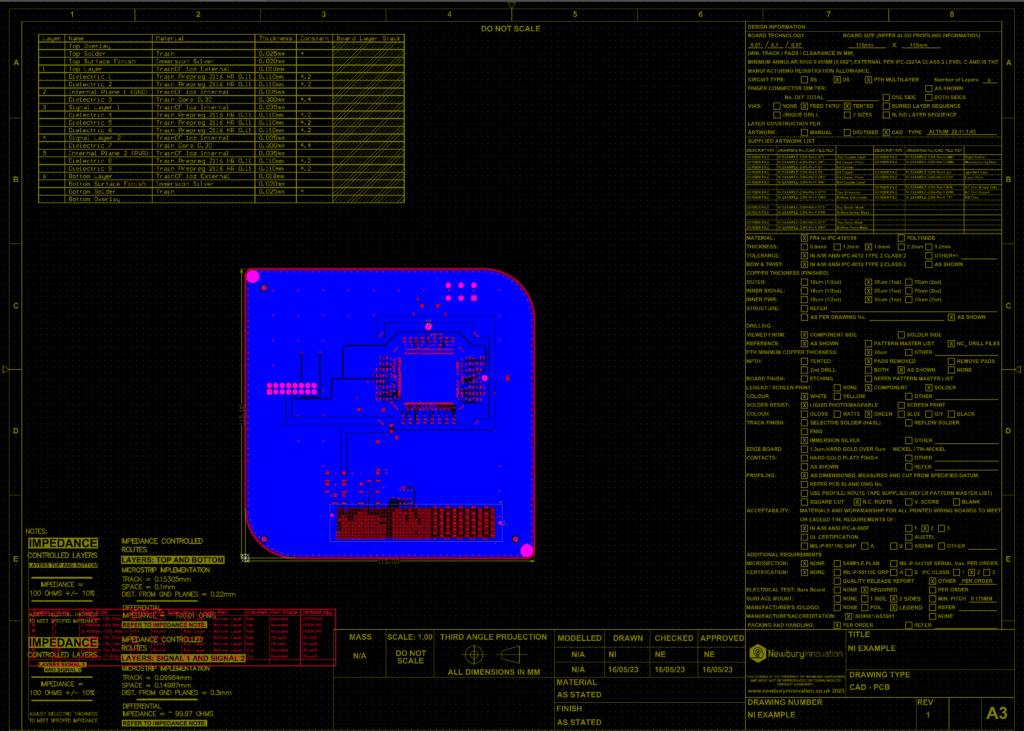
Technical advice for optimising the layout solution, whether single, double-sided or multilayer, flex or rigid-flex is available. Copper weight, laminate thickness and base material specification are recommended.
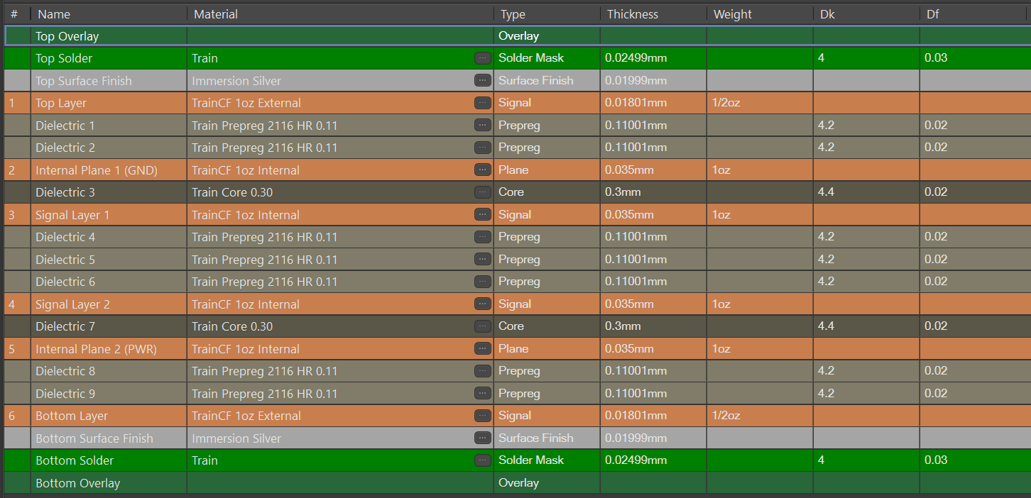
Existing designs in Altium Designer or Easy-PC can be modified directly. Other designs on alternative CAD platforms can be translated.
Production efficiency is optimised by the design of multi-panel production biscuits, including fiducials and break-out tabs, accounting for potentially adjacent overlapping components and compatibility with automated CNC de-pipping routing machine requirements. Panel rigidity will be designed in to ensure minimal bounce during automated SMD assembly.
![]() Client requirements are agreed and signed off in a technical specification document. This includes all aspects of the design such as a BOM, mechanical size and shape, thermal constraints, isolation, number of layers permitted, etc.
Client requirements are agreed and signed off in a technical specification document. This includes all aspects of the design such as a BOM, mechanical size and shape, thermal constraints, isolation, number of layers permitted, etc.
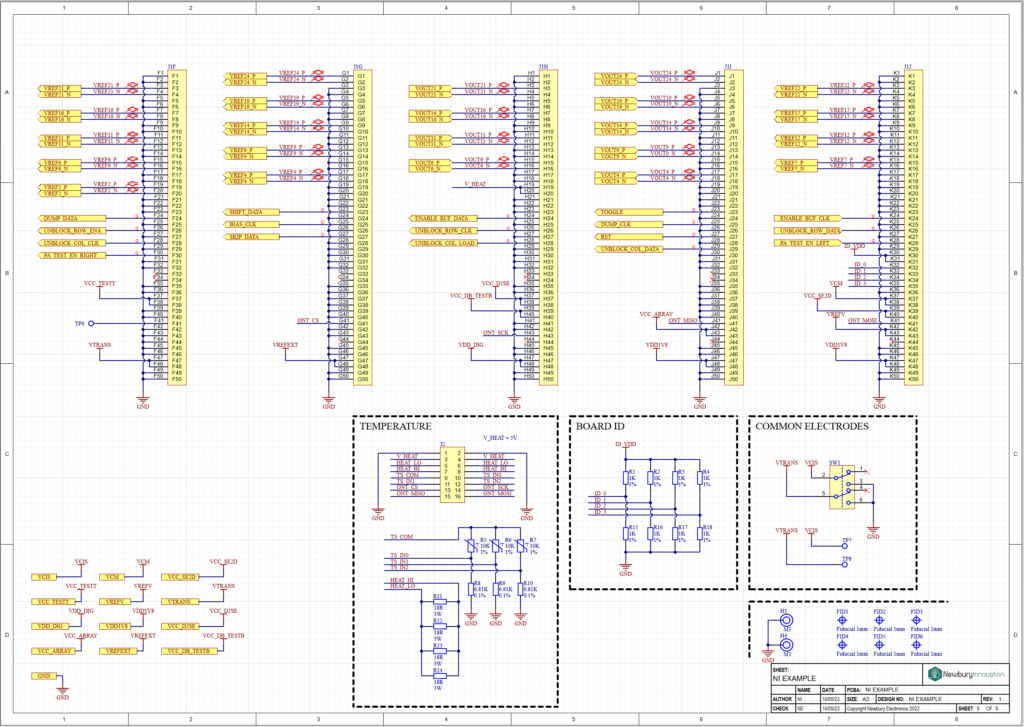
![]() A schematic design file is created, either by importation from OrCAD, Altium Designer, or Easy-PC or manually from client-supplied design notes showing the connectivity between every electronic component specified in the BOM. This is agreed and signed off with the client.
A schematic design file is created, either by importation from OrCAD, Altium Designer, or Easy-PC or manually from client-supplied design notes showing the connectivity between every electronic component specified in the BOM. This is agreed and signed off with the client.
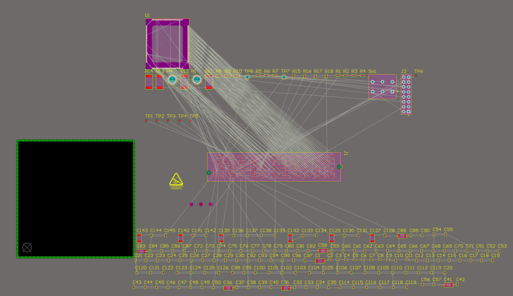
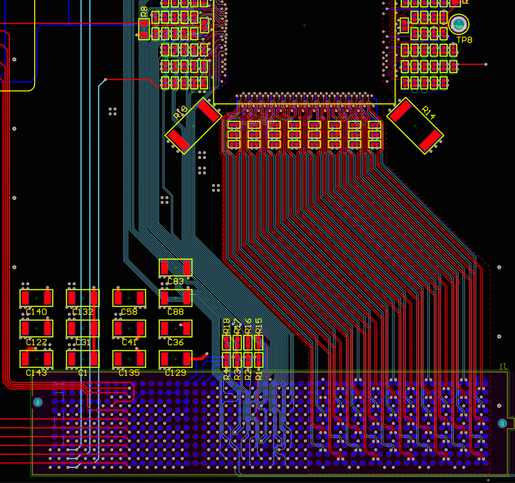
![]() We design the PCB layout to meet all the constraints specified and agreed with the customer. Modern CAD design software has many features that greatly facilitate design optimisation. Read More
We design the PCB layout to meet all the constraints specified and agreed with the customer. Modern CAD design software has many features that greatly facilitate design optimisation. Read More
![]() Design for production manufacture may be incorporated if required. This relates to the design of a suitable step & repeat production pallet and solder paste screen.
Design for production manufacture may be incorporated if required. This relates to the design of a suitable step & repeat production pallet and solder paste screen.
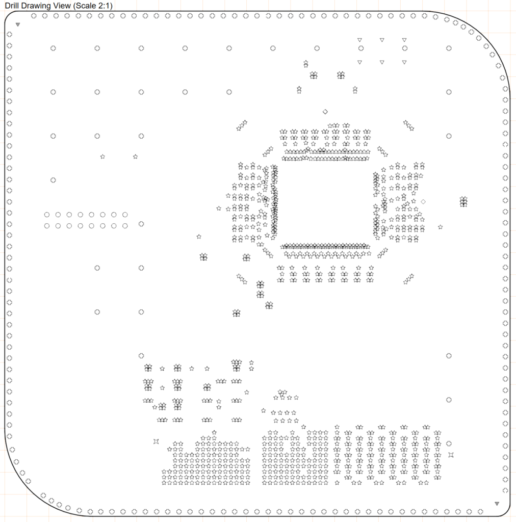
![]() Production data file generation creates all necessary files required for the fabrication and assembly of your PCB including an IPC compliant component library. We provide you with a complete project directory, including native Altium Designer or Easy-PC design files (as appropriate) , Gerber files, CNC drill data, assembly drawings, 3D modelling, fabrication drawings and reports, pick and place data, solder paste screen files, and BOM.
Production data file generation creates all necessary files required for the fabrication and assembly of your PCB including an IPC compliant component library. We provide you with a complete project directory, including native Altium Designer or Easy-PC design files (as appropriate) , Gerber files, CNC drill data, assembly drawings, 3D modelling, fabrication drawings and reports, pick and place data, solder paste screen files, and BOM.


Circuit schematic diagram or net list, preferably in OrCAD, Altium Designer or Easy-PC format.
Bill of Materials (BOM), including manufacturers’ part numbers.
Mechanical constraints drawing, including board dimensions.
Key components locations, e.g. connectors, mounting holes, display screens.
Relevant front panel, enclosure, or keypad drawings.
Board thickness, rigid or flex, or both, target number of copper layers and copper weight, base laminate material, power loadings, isolation, cross-talk, RF consideration, solder resist and legend colours.