About Newbury Electronics
Established in 1956, read about The Newbury Groups’ progress in PCB Manufacture & Electronic Design over the years..
Established in 1956, read about The Newbury Groups’ progress in PCB Manufacture & Electronic Design over the years..
when the business was established as a spin off from Newbury Engineering Limited, which had originally been formed by Major Ernest Lloyd, to undertake secondary machining on Zenith carburettors.
A factory at West Mills near the locks in the centre of Newbury was purchased, and Newbury Electronics developed its business in the manufacture of circuit boards, initially supplying the AWRE at Aldermaston and Leo Computers (ICL). The company was the subject of a number of acquisitions in the early 1970s before being acquired by AB Electronic Components PLC in 1972. Kevin Forder, joined the Company from AB Electronics in 1976 and was appointed Managing Director. Two years later, “plated through hole” (PTH) circuit boards were manufactured at Newbury for the first time, and CNC drilling machines were installed in 1979.
In 1980, the business moved nearby to a new custom built factory on the London Road Industrial Estate, which remains the company’s head office premises today. The following year Philip King, joined Newbury Electronics as the management accountant, and in 1987 partnered with Kevin Forder in completing a management buy out from AB Electronics.
Multilayer circuit manufacture started in 1989, together with the installation of the first CADCAM systems and AOI. In 1991, in-house laser photo-plotting began.
ISO 9001 approval was achieved in 1995. In the same year, the CEM (PCB assembly) division was founded, and the first brand new SMD pick & place machine was installed in 1999.
The online based PCB Train prototype PCB manufacturing service was also launched in 1999, and the ensuing growth led to the relocation of the assembly operations to the nearby River Park Industrial Estate.
Digital ink-jet legend printing was introduced for bare PCB production in 2003.
As the business expanded during the course of the decade, additional CNC drilling, electrical test, and SMD placement machines were purchased.
Laser cut solder paste stencil manufacturing operations started in 2010, and the company remains the only UK CEM to have in-house laser stencil cutting.
In-house X-ray inspection of PCB assemblies was established in 2013.
Laser direct imaging was introduced in 2014 for printing fine line copper plating resist masks.
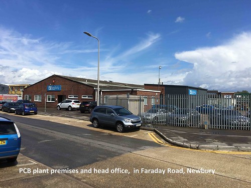
In 2015, a new plant-room was constructed at the PCB factory in Faraday Road to accommodate energy efficient compressed air and fume extraction equipment, and new de-ionised water and effluent treatment plant.
Tens of thousands of different types of pcb designs are manufactured for clients each year, many of which are also populated in-house. The company currently has nine fine pitch placement capable SMD pick & place machines.