
Sequential build up PCBs
We provide a wide variety of sequential build up PCBs incorporating blind and buried vias. Get the very highest quality printed circuit boards from an established UK manufacturer.
We provide a wide variety of sequential build up PCBs incorporating blind and buried vias. Get the very highest quality printed circuit boards from an established UK manufacturer.
Sequential build up (SBU) lamination is a PCB manufacturing technology where multiple layers of glass fibre base laminate and copper (generally double-sided copper and Hi Tg FR4 laminate) are bonded together sequentially creating a multilayer PCB with a variety of plated through holes, blind and buried vias providing interconnectivity between and within the layers.
The essential difference between regular multilayer pcbs and SBU pcbs is that the latter under-go multiple bonding processes, accumulating the layer count sequentially whilst the former undergo bonding all layers in one operation. It is good practice to bond SBU PCBs no more than four times.
Blind via diameter should be the same as its associated substrate thickness to facilitate down hole copper plating. To ensure the integrity of the bonding process, all blind and buried vias destined as internal layers are filled with conductive resin to eliminate air entrapment.
Blind vias are plated through hole connections that pass from an outside layer through to an internal layer copper pad. They do not pass all the way through the PCB like a conventional plated through hole. Blind vias are drilled by laser and typically have a diameter of 100 microns.
Buried vias are plated connections between the inner layers of a multi-layer PCB that do not emerge on either of the outer layers. Buried vias are created by drilling and copper plating the inner layer core (pairs) of a multi-layer PCB in the same way as a standard PTH PCB.
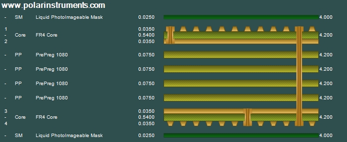
This is an example of a 4 layer PCB with blind vias between layers 1 and 2, & 3 and 4, together with through holes connecting all layers from 1 to 4. It is a typical build construction.
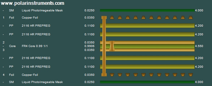
This is an example of a 4 layer PCB with buried vias between layers 3 and 4, together with through holes connecting all layers from 1 to 4. This is a typical build construction using commonly available laminations. We produce a wide variety of buried via pcbs. We recommend that your proposed construction is checked for compatibility with our manufacturing process before design finalisation. Send us details and ask us to quote.

Predicted impedance is checked against actual production outcomes by measurement of suitably designed test coupons using Time Domain Reflectometry (TDR) measurement instrumentation. Relevant PCB features are also measured with high resolution digital microscopy.
Ask us for advice on track widths, copper layer spacing, copper weights, and the base materials to achieve the impedance required. We use industry standard software to assist with impedance calculations and selection of appropriate PCB construction.
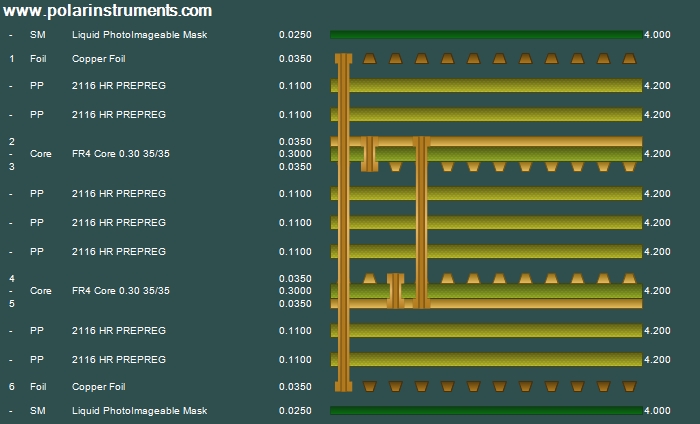
This is an example of a 6 layer PCB with buried vias between layers 2 and 3, & 4 and 5, together with plated through holes connecting all layers from 1 to 6 and 2 to 5. Once again, this build construction is typical.
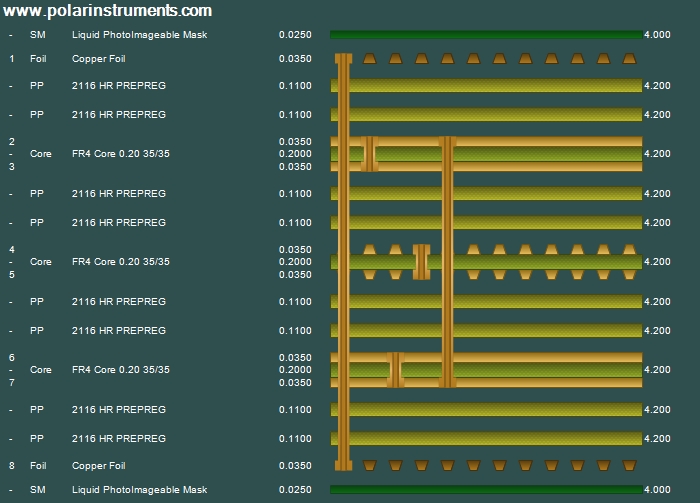
This is an example of a 8 layer PCB with buried vias between layers 2 and 3, 4 and 5, & 6 and 7,together with plated through holes connecting all layers from 1 to 8, and 2 to 7. Once again, this build construction is typical of its type.