
What is the Bare PCB Fabrication Process?
The bare PCB Fabrication process is often misunderstood to be of little importance however the slightest fault in the bare PCB will render any electronic assembly unserviceable. The PCB is usually the only bespoke component in an electronic system. It is the substrate upon which all the other components are commonly mounted. If it were a house, it would be the foundations. If the foundations fail, the house will collapse. It is wise to build your circuit on good foundations.
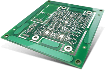
The PCB Fabrication Process
Manufacturing a PCB is a long series of sequential processes. A PCB fabricator takes copper clad fibre-glass and sequentially drills, prints masks, plates copper, tin, nickel, silver and gold, etches, bakes, chemically strips, cures fibre-glass and epoxy resin under vacuum and pressure, routs, and tests to produce a printed circuit board that should last a lifetime. It is a complex process interwoven with frequent quality controls required to attain lifetime zero defects.
Here is a brief overview of the PCB fabrication production process.
The PCB Fabrication Process
Orders are checked to ensure we have understood every aspect of our customer’s PCB design. Datafiles are checked for completeness, and correct version.
——
Queries are raised and resolved. Great care is taken to ensure that our production capability exceeds our client’s expectations. Order details are entered into the production planning and scheduling system.
Datafiles are checked for the correct issue version, and part number. PCB CAD layouts are design rule checked for every aspect which will impinge on manufacturability and quality. Our extensive experience in assembling PCBs ensures we can review customer designs with a keen eye for design for manufacturability (DFM).
——
Any queries that arise are referred to clients and resolved accordingly. Production tooling with handling frames and step and repeat is generated for drilling, routing, copper layers, solder resist layers, and legend layers, solder paste screens plus electrical test tooling. These will all be appropriate datafiles which are saved to the tooling database under a tool number. The entire PCB production process is driven by software tooling.
We hold large stocks of PCB laminate, all in pre-cut blank sheets which are available directly for issue to production.
Blanks are loaded on to auto-load high-speed, auto-drill change CNC drilling machines. Holes are drilled for via connections, and for through hole technology components. Monitoring devices on the drilling machines check for correctness of drill selection and detect drill breakage.
Drilled PCB blanks are passed down a conveyorized line which lines the holes with a thin layer of carbon which will act as the cathode in the electrolytic copper plating process.
Drilled PCB blanks are laminated with photosensitive dry film plating resist, and digitally imaged by automatically self-registering direct imaging machine. No photographic films are used. Consequently, registration of drilling to copper lands is unmatched. The image is developed in a conveyorized dry film processing machine.
Imaged blanks are electrolytically copper plated using periodic pulsed plating, a technique which plates copper evenly both down small holes and on the surface of the tracks.
——
Frequent measurements are taken to ensure every panel has the correct amount of copper plated down the holes. A layer of tin is plated over copper tracking, and this tin metallic layer will become the etch resist layer when the photo-mech dry film plating resist is stripped.
In a conveyorised process, the photo-mech plating resist is stripped, and followed by the etching process. The etching process is closely monitored to ensure neither under or over etching of the PCB blank.
For circuits requiring multiple layers such as 4,6 ,8,10 or 12-layer PCBs, individual pairs of inner layers will be printed and etched. Copper tracking needs to be treated to create a surface upon which the resin can bond, and this is achieved by passing the inner layers down a conveyorized black oxide line.
——
The layers are assembled into “books” with fibreglass and resin prepregs being interleaved between the layers to create the required insulation gap between layers and the appropriate overall PCB thickness. The books are spot welded together to maintain inter-layer registration prior to bonding at high temperature under high compressive pressure in a vacuum chamber. This process cures the resins, and eliminates any air bubbles in the stack. Multi-layer blanks return to the drilling process and are processed similarly to double sided PCBs to print and finish the outer layers.
Photo-imageable solder resist of the appropriate colour is coated over both sides of the PCB panels and partially cured in a low temperature oven.
——
The solder resist image is printed, once again using a digitally driven direct imaging machine, self-registering giving excellent pad to resist registration every time. The image is developed in a solder rest processing machine. A final bake in an oven cures the resist resins.
Exposed copper pads are finished with either immersion silver, or electroless nickel immersion gold (ENIG) according to customer requirement. Coating thickness is verified using an X-ray fluorescence instrument.
The legend is printed using a high speed and high-resolution digital inkjet printer, which cures the ink as it prints.
PCB panels return to the drill shop where they are routed into individual circuits.
All PCB circuits are 100% electrically tested using high speed flying probe machines.
Finished circuits are vacuum packed in anti-static bubble wrap, packed and despatched.
Every process is logged on the computer tracking system. All materials are fully traceable to their source.
At every stage of the process, PCB panels are closely inspected. Depending on the complexity, automated AOI systems will be used during the PCB production process and in final inspection.
Finished PCB’s are finally checked and packed in vacuum heat-sealed antistatic bubble wrap and shipped, as per client instructions.