The Printed Circuit Board Assembly (PCBA) Process
[vc_row][vc_column][vc_column_text]
Printed circuit board assembly, or PCBA, is the process of soldering electronic components onto a PCB. Here we give you on overview of the SMT, pick-and-place, and inspection techniques that take place in our assembly facility during the electronics assembly process.
Step 1: Request For Quote
The PCBA process starts with a quote estimating the cost of parts and assembly according to a customers request. Our team check the requirements against our quotation carefully to ensure that everything that is quoted has been ordered and that everything ordered has been quoted for. At Newbury Electronics we aim to respond to a request for quote within 24-48 hours.
Step 2: Buying & Bill of Materials (BOM)
To begin the purchasing process to put together a kit of parts, we upload the bill of materials onto our production control system. Our team checks that we have all the data required to make the electrical product and prepare documentation for production. If there are any queries, we get back to the customer straightaway. Our buying team not only source the best price for the parts from our suppliers but they take into account extra quantities required for lead ins or spares to account for any scrap that might arise during the production process. The packaging of components is also considered at this stage, as some may need to be on wheels while other parts may need to be loose.
Step 3: ESD Precautions
During the course of the electronics assembly process, components are susceptible to damage through electrostatic discharge. In order to avoid this risk, Newbury Electronics take extensive ESD precautions. The floor is conductive and earthed and all staff is required to wear conductive wrist straps and footwear, always checking that their ESD protection is working satisfactory on a test set.
Step 4: Electronic Component Kitting
Kitting is at the heart of the electronics assembly process and involves producing production ready kits and ensuring all parts are delivered to the right people.  This process also checks that the quantities are correct to avoid any shortages later down the line. Every part that arrives is checked against the Bill of Materials (BOM) and often parts will need to be examined within their protective packaging, making note of any moisture sensitive parts. Any identified are repacked with vacuum resealing moisture resistant bags to exclude air and reseal them against the ingress of humidity. Once our team is satisfied that all components are correct they are labelled up.
Step 5: Dry Cabinet Storage
Many electrical components are susceptible to the ingress of moisture and so we use a humidity-controlled dry cabinet to store moisture sensitive components. The dry cabinet keeps the components at a relative humidity of around 3% which is sufficient to keep them dry enough to solder later on in the PCBA process.
Step 6: CAD/CAM Programming
Nearly all component assemblies require us to prepare the SMD placement programmes which will guide the operator as to which components go on the feeder and in what position. Our CAD/CAM programming team takes the client data and converts it to computer programmes that are readable by our SMD machines and our AIO machines.
Step 7: Laser Cut Solder Paste Stencils
Laser cut stencils are used to aid the application of solder paste to surface mount component pads during the PCBA process. They allow assemblers to apply solder paste only where components will sit in the finished circuit board. With our own solder past stencil machinery, Newbury Electronics has an advantage over other UK companies. Access to our own technology enables us to cut laser stencils very quickly without having to wait on a third party. This is highly effective and cost-saving as it means that our customers don’t incur additional charges for our stencil service.
Step 8: Solder Paste Printing
Before the surface mount parts are placed by the SMD machines, we screen print solder paste onto the surface of the PCB pads. It’s a crucial step in the PCB production as the quality of solder paste can affect the performance and reliability of the surface mount assembly. Solder paste has the consistency of butter and this is just thick enough so that when the surface mount parts are placed on the surface of the pad they will stay in position.
Step 9: SMD Pick & Place
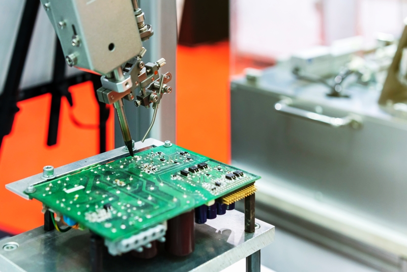
After the solder paste has been applied to a board, the PCBA process moves onto the pick-and-place SMD assembly machines. We have 9 here at Newbury Electronics including 6 Yamaha iPulse M20 Pick and Place machines. They are programmed to pick the parts from reels and place them onto the surface of the PCB in pre-programmed locations. These robots can do this at a rate of 20,000 parts an hour. The board is then moved onto a conveyor belt to process through a solder reflow machine, a large oven that fuses the solder paste into a permanent solder joint to connect the SMDs to the PCB.
Step 10: First Article Inspection
Whilst the SMD assembly machines are extremely productive, it’s essential that the first boards out are tested for errors or misalignments. Alongside manual checks we inspect the PCBs on a small AOI machine that checks that the correct part is placed on the right orientation at the right coordinate.
Step 11: Surface Mount Technology
For larger batch sizes, which may be quantities of 25 or 50 pieces upwards (and certainly when we have to manufacture 1000 or more), we’ll run these production runs on our high capacity SMD assembly lines for quality and efficiency. The first SMD station in the line is capable of placing 20,000 parts an hour.
Step 12: Automatic Optical Inspection
(AOI) Automatic Optical Inspection is a quality control method essential for large batches of PCBAs. AOI machines take an optical image of the circuit board under examination using high-powered cameras placed in different angles. It compares the image of the components with those in its memory so that it can detect any misplacement of parts or missing components. This is done at high speed ensuring that a high quantity of PCBs can be processed quickly.
Step 13: Hand Placement of SMD Parts
Most components these days are placed by service mount assembly machines, but there are always some hand placed components during PCBA too. Hand placed components could be parts that have to be inserted down holes and the wires cropped off, or components that have arrived loose in a bag.
Step 14: Wave Soldering
Wave soldering is a bulk process used to solder printed circuit boards quickly during PCB assembly. Using a wave soldering machine, PCBs are treated with flux, preheated and immersed in liquid solder. Circuit boards pass over a wave solder so that all of the joints on the underside of the board are soldered at the same time.
 Step 15: X-Ray Inspection
Many components have their solder joints under the body of the part, for instance ball grid array’s or QFN devices. If that’s the case then AOI or visual inspection cannot check the quality of the joint. Therefore, an X-Ray inspection machine is required for quality control.
Step 16: Flying Probe Test
The flying probe test machine is a sophisticated test instrument which measures the value of components in circuit. It can test a circuit board at the rate of about 5 tests a second, and the machine will measure resistance, capacitance and inductance, and various voltages and frequencies. This way the value of every part on the circuit board can be checked.
Step 17: Functional Test (FCT)
At the end of the PCBA process, a range of final tests are carried out. A functional test is carried out where we power up an electronic assembly and test whether it functions in accordance with the customer specification. Some parts on a circuit board can’t be inspected by earlier AOI or X-Ray inspections, and so a final inspection by eye is also required to ensure the quality of the final product.
See How PCB's Are Assembled
Check out our video for a full PCB assembly factory tour and watch the electronic assembly process in action.[/vc_column_text][/vc_column][/vc_row]

