
Surface Mount Technology
With state of the art machinery and rigorous implementation of process control, at Newbury Electronics, we offer an unparalleled SMT assembly service for a wide variety of industries.
With state of the art machinery and rigorous implementation of process control, at Newbury Electronics, we offer an unparalleled SMT assembly service for a wide variety of industries.
Surface mount PCBs assembly occurs when electrical components (surface-mount devices) are machine picked and mounted directly onto the surface of the PCB. During this process, thousands of electrical components are attached and connected to their contact pads using reflow soldering.
Nowadays, the majority of electronic assemblies are designed using surface mount components and technology. This is in part because SMT allows for increased quality and a reduction in manufacturing costs due to the high degree of automation.
However, surface mount assembly presents challenges to manufacturers which must be met through the astute selection of appropriate production equipment. This expertise allows us to design products which are completed in one pass down an automatic SMD assembly line without any extra hand assembly work other than to snap the circuit board into a moulded enclosure. Over the years, our electronic assemblers have optimised their methods to achieve a highly efficient SMT process that is second to none across the UK.
For a PCB assembly quote or to discuss your requirements, please use our online form.

A key process in surface mount assembly is the design of the solder paste stencil. It is paramount that the quantity of solder paste deposited on each pad is repeatable and precisely controlled. We consider this to be so important that we precision cut our stainless steel stencils by laser using our own in-house industry-standard laser cutting machine. Modifications and improvements to production stencils can then be made at low cost within hours as and when required, minimising delays and waiting time.
For the solder paste printing process we utilise modern printing machines incorporating automatic load and unload to reduce handling. Using automatic camera fiducial registration we then ensure perfect placement of solder paste every print and with automatic under stencil cleaning we minimise cross-contamination of surplus solder paste between prints, which is a major potential cause of faults. Finally, in machine automatic optical inspection (AOI) of the solder paste print takes place to check the height and size of each pad printed.
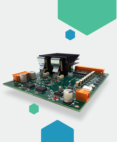
Surface Mount Device or Technology components (SMD / SMT being interchangeable) are now at the heart of all electronic systems and these parts do not require connections made by wires inserted into drilled holes. The definition of an SMD or SMT part is a component whose exterior connections are flat copper pads and arranged to sit on a mirror image set of plane copper pads (being the SMD footprint) printed on the PCB surface. The SMD connections may alternatively be made by a wire leg which has a bent section which will sit flat on the PCB copper pad. The SMD part is placed very accurately by the SMD placement machine at the exact centroid of the footprint, with the correct rotation, upon a typically 25-micron layer of solder paste, previously screen printed upon the bare PCB SMD pad.
We manufacture many small batches and benefit from having SMD placement machines with interchangeable feeder carts. Carts can be rapidly moved between machines and storage as production schedules demand. SMD feeder carts are set up offline without interrupting SMD machine production, matching component reels and feeders according to the SMD placement programme.
At Newbury Electronics we are equipped with 10 lines of the latest model SMD placement machines, capable of placing a wide variety of part sizes from the smallest type 1005 SMD parts (0.4mm x 0.2mm) up to large SMD connectors (dimension 30 mm x 10 mm).
Our AOI machines are of the latest technology and equipped with high resolution 2D downward looking cameras combined with instruments that 3D map the surface of the assembly. 3D AOI is a remarkable step forward in electronic assembly inspection technology. For example, 3D data enables the measurement of the amount of solder on each SMD solder pad in an instant.
Likewise, “lifted” legs on gull-wing type components can easily be identified. This pernicious fault arises where a QFP leg is minutely bent upward so that solder joint is not quite made during the reflow process. Poor fusing of a BGA‘s solder balls causes it to “capsize” slightly, and this can be detected by 3D data.
Our Takaya flying probe test machine is particularly capable of surface mount technology. The machine measures resistance, capacitance and inductance through four lead screw driven probes. We develop test programmes from the pick & place machine programmes which give the location of the parts, and the BOM which identifies the technical measurement that is applied to confirm that the value of the parts placed are correct. We also use Diode and transistor checks.
Developed in the 1960s, surface-mount technology is one of the methods for electronic printed circuit assemblies currently performed by industry experts. Nowadays, SMT is one of the most widely used component assembly technologies for offering a lower-cost and faster solution than other similar methods.
With surface mount technology, components are mounted directly onto the surface of the PCB. During this process, thousands of electrical components are attached and connected to their contact pads using reflow soldering.
Like any project, it starts at the design stage. Depending on the sizes of the components and the capabilities of the machinery used it is possible to complete the design of the product in one pass down an automatic SMD assembly line without any extra hand assembly work other than to snap the circuit board into a moulded enclosure. At Newbury Electronics, we work with the latest machinery, capable of placing a wide variety of SMD sizes, from 0.4mm x 0.2mm up to 30 mm x 10 mm, making the process far more efficient.
Before placing the components on the board, solder paste stencil is produced to secure them and it is paramount to ensure that the quantity deposited on each pad is repeatable and precisely controlled. The solder paste printing process can be done through specialised printing machines incorporating automatic load and unload to reduce handling.
On the next step, the printed PCBs proceed to the pick and place machines for the components to be placed on them and then straight through to the reflow soldering oven.
During the reflow soldering process, the assembly is heated in a controlled manner causing the solder paste to melt and the components to be electrically secured to the printed circuit board. This is achieved either by convection or by vapour phase reflow.
And finally, we have the inspection of the boards. At Newbury Electronics we use automatic camera fiducial registration to ensure perfect placement of the solder paste, automatic optical inspection (AOI) to check the height and size of each pad printed, Takaya flying probe test machines to measures resistance, capacitance and inductance, transistor checks and other inspection equipment.
Before surface mount technology came around, through-hole technology (THT) was the main printed circuit board assembly process used. However, SMT allows for high-speed production, permitting higher-density circuits and making through-hole mounting rarer and even discouraged sometimes.
It is far more efficient to machine assemble an electronic circuit if it is completely populated with surface mounted components. Leaded parts or through-hole components, on the other hand, are laborious to fit. They need lead trimming and bending, hand placement, further trimming and hand soldering. SMDs are simply machine picked and placed from a reel.
Yet, this technology is still used for some applications which is why we also offer through-hole assembly services. It involves component leads being placed into drilled holes on bare PCBs making it ideal for products that require stronger connections between layers.