

5G And PCBs – What You Need To Know
Are you 5G-ready?
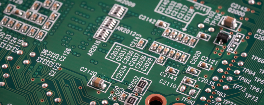
With 5G accessibility becoming more widespread, manufacturers must rethink their approach to PCB design and draw on specific techniques to ensure that what they produce is optimised to support 5G’s enormous potential.
Read our blog to explore everything you need to know about 5G and PCBs as this new technology begins to take hold.
What Is 5G, And Why Will It Affect PCBs?
5G has been available since 2019 and is the fifth generation of mobile broadband technology. As the follow-up to 4G, it is notable for having greater connectivity, higher speeds and much lower latency than its predecessor. The 5G network achieves these advantages by operating at higher frequencies, extending its reach to the previously unexplored millimetre wave (mmWave) band.
From a consumer perspective, all of the above means faster response times, a more reliable user experience and almost faultless coverage. For PCB manufacturers, 5G’s high frequencies and ultra-responsiveness require certain tweaks to circuit board design. Failure to make these changes could mean missing out on 5G's incredible benefits.
What Changes Do I Need To Make?
At the time of writing, there are several things you can do to enable your PCBs for 5G. These include embracing new production methodologies and making small changes to your existing ways of working.
Here are a few recommendations.
- Use a semi-additive fabrication process (mSAP): As PCB design becomes even more complex under 5G, designers will begin to rely on high-density interconnect (HDI) PCBs with thinner traces. The danger with this is that thinner traces may lead to signal loss and impact overall performance. Mitigate this issue by using an mSAP, which will allow you to form straighter, more precise traces that won’t jeopardise signal integrity.
- Select materials wisely: 5G’s high-speed signals generate enormous amounts of heat, which can lead to PCB breakdown. To reduce this risk, manufacturers must select board materials wisely and opt for those capable of dissipating heat effectively. This includes choosing substrates and materials with low dielectric constants. 5G-enabled devices are also likely to be compact, so you should expect to be using more flexible PCBs than rigid ones.
- Switch to automated optical inspection (AOI): Identifying issues in PCB design and performance is a fundamental part of the printed circuit board creation process. Switching to automated optical inspection systems when creating 5G-ready designs can speed up these tasks, and will enable you to detect errors and correct mistakes with minimal input from employees. Optimising your inspection processes as 5G becomes more of a concern will also help free up your floor space and resources.
The Time For 5G-Ready PCBs Is Now
At Newbury Electronics, we are constantly refining our PCB production processes in order to stay ahead of the curve. The advent of 5G is something we have long anticipated, and we will continue to make adjustments as our understanding of this technology progresses.

To find out more about what we do, and to create a PCB that is fully optimised for 5G technology, please get in touch with us today.