
A Step by Step Guide to the PCB Fabrication Process
A Printed Circuit Board (PCB) is a thin board that connects electronic components. Used in almost every electronic device that you can think of, PCBs have developed in complexity over time whilst delivering a more compact design. So, how is a printed circuit board produced? Find out here as we break down the PCB Fabrication process.
Step 1: Quote & Order
Every manufacturing job at Newbury Electronics starts with an order that we have received online or over the phone. It is then the job of our sales team to ensure that all of the information we receive from the customer is sufficient for us to make the printed circuit board. For standard construction PCBs, we only require a brief description of the nature of the PCB, together with Gerber and CNC drill file data. For multi-layer PCBs, we require detailed material specifications and layer build-up drawings. Once our team is happy with the specification, the details are passed onto our CAD CAM department to process the data for production.
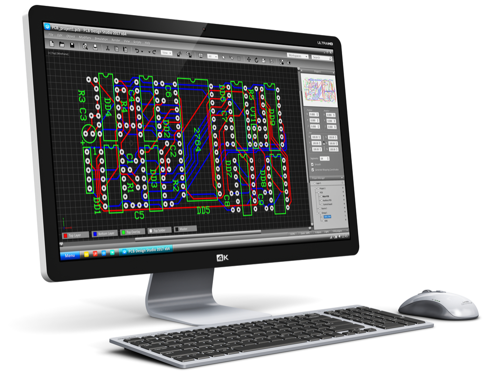
Step 2: CAD/CAM
The CAD CAM tooling process is a crucial step in the PCB fabrication process to ensure that the data we prepare can be manufactured. Our engineers take customer data and create PCB production tooling using the latest CAD CAM software tools, with complete design rule checking. Part of the data that our engineers produce is film work data, which can be plotted on our laser plotter and printed onto silver halide photography.
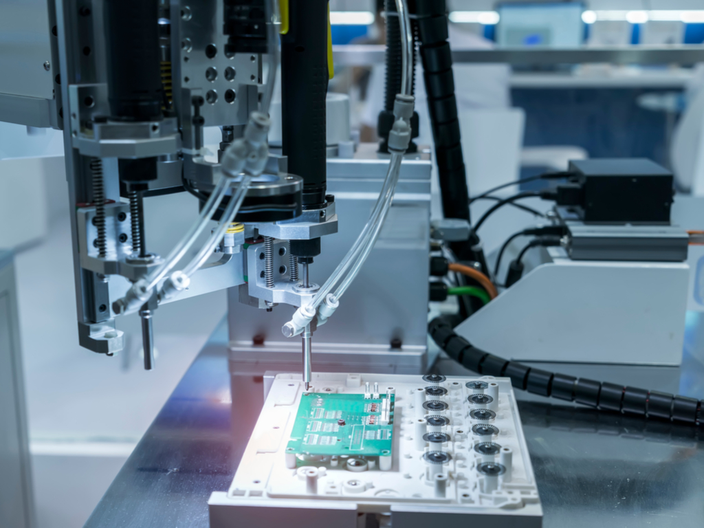
Step 3: Drilling
Once the PCB design has been verified, the next step is to drill via holes in the copper blanks. Printed circuit boards need holes to both mount components and to connect the top and bottom layers at different points. The location of the holes will depend on the design of the circuit board. The PCBs are drilled on an automatic load and unload drilling machine that is linear motor-driven in the x, y and z axis. The machine contains a vast number of drills to accommodate all sizes that may be required during the course of the drilling, which could take a few days. A typical PCB production panel will have multiple circuits as our cost-effective setup allows us to produce up to 10 or 11 circuits at the same time on the same sheet.
Step 4: Multi-Layer Vacuum Lamination
The multi-layer bonding process creates the blank on which you print the outer layers of the circuit board. The inner layers, which have already been prepared with a printing tech process, are bonded using prepregs in the multi-layer press. Platens loaded with the inner layer blanks are loaded onto the lamination press and heated with oil at about 185 degrees for about two hours to cure the laminate.
Step 5: X-Ray Hole Drilling
After the multi-layer bonding process, you’re left with a blank with copper sheets on either side. The patterns within that blank cannot be seen and so drilling through the blank is required to target the pads on the inner layers. The X-Ray hole drilling machine is used for drilling precision holes in the multi-layer blanks. It x-rays targets in the corners of the blank and calculates the best position for two registration holes on the centre line of the blank. This process ensures that we drill accurately through the inner layers.
Step 6: The Black Hole Line (Direct Metallisation)
During PCB fabrication, the direct metallisation line is also known as the black hole line. In this process, we put a layer of carbon down the barrel of the holes of the PCB and the carbon becomes the cathode in the electrolytic plating process, so that we can plate a thin layer of copper down the holes of the printed circuit board. The copper-coated walls allow electricity to be carried from one side of the circuit board through a plated hole to the other side of the board, or between different layers.
Step 7: Laser Direct Imaging
The next step in the process of making a PCB is laminating, printing and developing the artwork of the circuit board through precise laser direct imaging. Our Photomech department uses a laser machine that scans the surface of the blank and efficiently prints the image of the board onto a photosensitive film.
Step 8: Electrolytic Copper and Tin Plating
At this point in the PCB fabrication process, the blanks have been drilled, carbon has been put down the holes and we’ve applied the plating resist. So we’re now ready to electrolytically plate the circuit boards. The blanks remain in the electrolytic copper tanks of the plating line for about an hour to complete the plating process; they are then carried over to the tin tank which takes about a further ten minutes. We use a periodic reverse pulse plating process (not a DC plating process), which means that for a few milliseconds a high current is applied in the reverse direction which improves the throw rate of the copper down small holes.
Step 9: The Strip-Etch Strip Line
The developed board will now move on to the next step which involves resist stripping, etching and tin stripping. Once the board has been plated, the photoresist is no longer required so we use a machine to completely strip the plating resist from the panels. The second stage in the line is the etching process to efficiently remove all unwanted copper from the PCB. As the only function of the tin was to protect the copper tracks and plated holes, the final stage is to strip the tin from the surface of the panel.
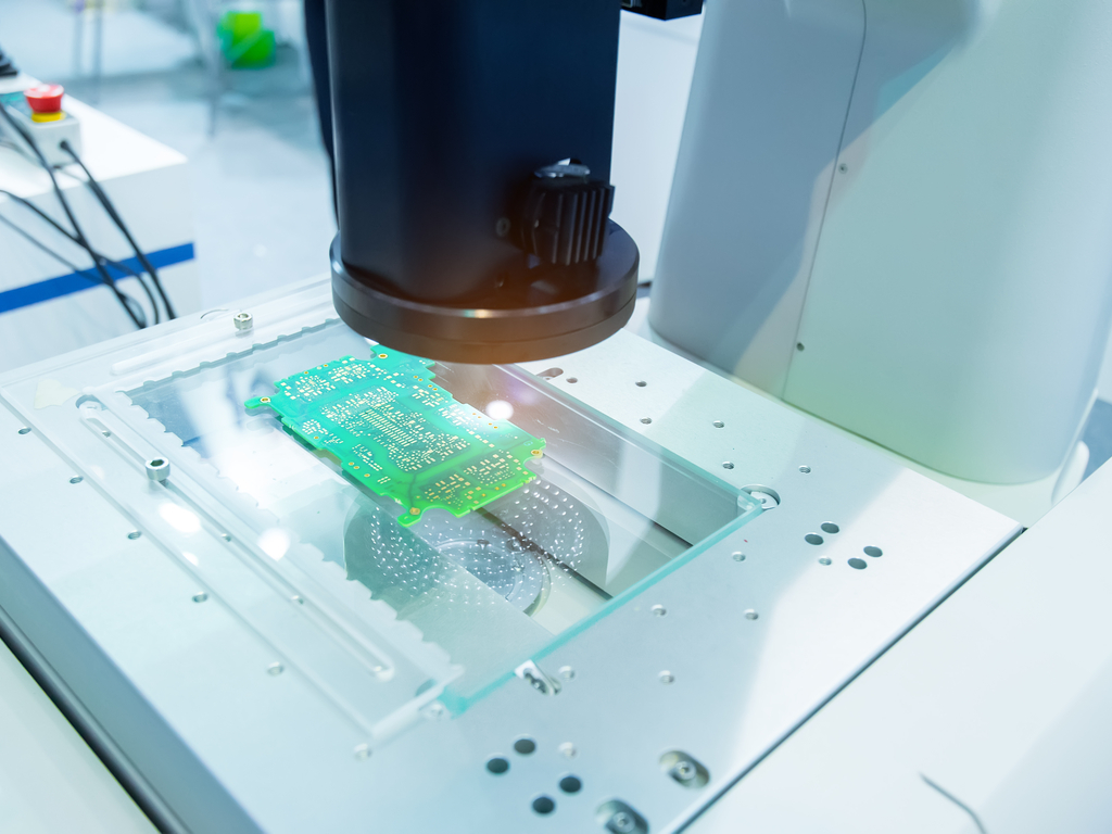
Step 10: Automatic Optical Inspection
Automatic or automated optical inspection (AOI) is a key part of the manufacturing process where the circuit boards are scanned by a camera and compared to CAD data previously created. AOI can identify any differences that an operator will check and see whether an error identified is significant or not. This step ensures the high quality and accuracy of the board leaving the production line.
Step 11: Solder Resist
Following the strip-etch strip process, the copper blanks require a solder resist (a permanent resin-based coating) to be applied. Solder resist is photoimageable ink, usually green in colour, that is applied over the entire surface of the PCB. Both sides of the board are flood-coated and tack-dried for a short period of time.
Step 12: The Immersion Silver Line
To provide a good solderable finish in the PCB assembly process, next we apply a very thin layer of silver line across the surface of the pads.
Step 13: Legend Printing
Legend printing is the white ink that you generally print on one or both sides of the PCB. It contains component designators and identifies where the parts are placed, important for the assembling process. We print the legends using an inkjet legend printer, which is an industrial version of a standard desktop inkjet printer.
Step 14: Drilling & Routing
Once the legends have been printed, the boards must be separated by routing the individual circuits out of the panel. So the PCBs are returned to the drill shop and put on the same drilling machines as used earlier in the process. This prepares them for assembly later in the manufacturing process.
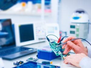 Step 15: Electrical Test

In order to verify that a multi-layer board will work, every circuit board is electrically tested. Our machines measure the continuity of every net on the circuit (data prepared by our CADCAM department) and they check for isolation by measuring the capacitance of each net. It will double-check any net that has a similar capacitance to make sure they’re isolated.
Step 16: Final Inspection
During the course of the PCB production process, the circuit boards are returned to inspection for a careful check that they are of high quality. The final inspection is where we take one last look at the circuit boards before we dispatch them.
Step 17: Packing & Despatch
After all the production processes are complete, we’re left with the packing process where we make sure that the completed circuit boards are packed and despatched to the correct customer delivery address.
Step 18: Waste Management
We consume about 50 cubic metres of water in the PCB manufacturing process and it all has to be treated before we can discharge it to the drain. We treat it in a tower that contains about two tons of activated carbon and the effluent that passes through the tower remains in contact with the carbon for about 30 minutes. This takes out all the heavy metals. After it's treated, the water is purer than when it arrives at our factory in the mains water supply! All of our scrap materials are recycled, from steel scrap to copper brasserie, so nothing goes to waste. Anything we can’t recycle gets collected each week and goes to a combined heat and power generation plant where it gets incinerated and produces electricity.
See How PCBs Are Made
To watch how PCBs are made in a real and functioning PCB factory, check out the video on our YouTube channel for a full factory tour at Newbury Electronics. What’s next? Find out how a PCB is assembled with our guide to the PCBA process.